PNP Transistor: Operation and Use as a High-Side Switch
PNP structure and operating regions, complete design of a high-side switch driven by a 5 V or 3.3 V microcontroller, and data for the 2N3906, BC557 and 2N2907A.

The PNP BJT is the complementary sibling of the NPN BJT transistor (in Italian): same physics, same three operating regions, but with polarities and current directions reversed. To conduct, the base must sit about 0.6–0.7 V below the emitter, and the emitter is usually connected to the positive supply rail. It is precisely this property that makes the PNP transistor as a switch the natural choice on the positive side of the load, the so-called high-side switch.
In this guide we first take a concise look at the structure, symbol and operating regions of the PNP, following the conventions of the NPN article. The core of the article, however, is the use of the PNP as a high-side switch: a complete design example (load, collector current, minimum hFE, base current with an overdrive factor, base resistor and base-emitter resistor) and driving it from a 5 V or 3.3 V microcontroller through an NPN, which is essential when the emitter runs at a voltage higher than the logic supply. We close with the datasheet figures of the 2N3906, BC557 and 2N2907A, including the pinouts that must not be confused.
PNP BJT structure and symbol
The PNP is made of three semiconductor regions in a P-N-P sequence: a heavily doped P-type emitter, a very thin, lightly doped N-type base, and a larger P-type collector, designed to withstand the reverse voltage and dissipate power. Emitter and collector are both P-type but they are not interchangeable: if you swap them the transistor still conducts, but with very low gain and with parameters that are not guaranteed. For the meaning of P and N doping, see N-type and P-type semiconductors (in Italian).
When the base-emitter junction is forward biased, the emitter injects holes into the base. Holes are majority carriers in the emitter, but they cross the N-type base as minority carriers: because the base is thin, only a small fraction recombines (and this recombination makes up most of the base current), while most of them reach the reverse-biased base-collector junction and are collected by the collector. The mechanism is identical to that of the NPN, with holes in place of electrons.
Symbol, current directions and sign conventions
In the PNP symbol the arrow is on the emitter and points toward the base: it shows the conventional direction of current in the forward-biased base-emitter junction. As a consequence, in the PNP the current enters at the emitter and leaves from the base and the collector, the opposite of the NPN.

Kirchhoff’s current law also holds for the PNP, and the static gain is the ratio between the currents:
\(I_E = I_C + I_B \qquad h_{FE} = \frac{I_C}{I_B}\)
PNP datasheets give voltages and currents with a negative sign (VCEO = −40 V, IC = −200 mA, VCE(sat) = −0.4 V): this is simply the result of the reference convention, the same one used for the NPN, applied to a device that works with opposite polarities. In calculations it is easier to reason with positive quantities by swapping the order of the subscripts: VEB = VE − VB instead of VBE and VEC = VE − VC instead of VCE. In this article we will always use positive VEB, VEC, VEB(sat) and VEC(sat) and current magnitudes, exactly as the NPN article uses VBE, VCE, VBE(sat) and VCE(sat).
NPN to PNP correspondence (positive values)

NPN                      PNP
VBE  ≈ 0.6…0.7 V         VEB  ≈ 0.6…0.7 V     (base below the emitter)
VBE(sat)                 VEB(sat)             (datasheet: −VBE(sat))
VCE(sat)                 VEC(sat)             (datasheet: −VCE(sat))
VCEO = 40 V              VCEO = −40 V         (same limit, opposite sign)
emitter to ground        emitter to positive
low-side switch          high-side switch
PNP operating regions: cutoff, active region and saturation
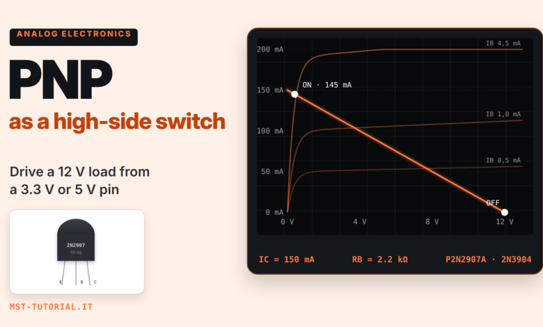
The PNP has the same three operating regions as the NPN, defined by the state of its two junctions. The chart shows the output characteristics IC = f(VEC) with the load line of the example design we will develop later (12 V, 80 Ω).

| Region | B-E junction | B-C junction | Potentials | Behavior | Use |
|---|---|---|---|---|---|
| Cutoff | not biased (VEB < about 0.5 V) | reverse | VB ≈ VE | IC ≈ 0 (leakage currents only, tens of nA) | open switch |
| Active region | forward | reverse | VE > VB > VC | IC ≈ hFE · IB |
amplification |
| Saturation | forward | forward | VC close to VE | IC set by the load, VEC(sat) ≈ 0.1–0.4 V | closed switch |
In cutoff the base is at the same potential as the emitter and the transistor is off. In the active region the collector current is controlled by the base current through hFE, which however varies with IC, VEC, temperature and from part to part: this is why an amplifier is designed with feedback rather than relying on a precise gain value. In saturation the base-collector junction is forward biased as well: the collector moves to within a few tenths of a volt of the emitter, and the current no longer depends on IB but on the external circuit.
In switching applications the transistor works only at the two ends of the load line: the OFF point (VEC ≈ VCC, IC ≈ 0) and the ON point in saturation. The transition through the active region must be fast, because that is where the transistor dissipates the most. For example, a 2N3906 in the active region with VEC = 10 V and IC = 50 mA dissipates 0.5 W: with RθJA = 200 °C/W the junction would rise 100 °C above ambient, that is 125 °C at 25 °C ambient, too close to the 150 °C limit.
The PNP transistor as a high-side switch
In the high-side configuration the PNP emitter is connected to the positive supply, the collector feeds the load and the other end of the load goes to ground. Compared with the NPN low-side switch (load between the positive rail and the collector, emitter to ground), the advantage is that the load, when off, stays referenced to ground and does not “float” at the supply potential: this is the preferred solution when the load shares a ground with other parts of the circuit (modules, sensors, sections of a system powered on demand, common-cathode LED strips) or when you want to remove the positive supply from a section of the circuit entirely.
The drive principle is simple:
- OFF: the base is brought to the emitter potential (VEB = 0). A resistor RBE between base and emitter guarantees this condition even when the control signal is floating, for example during microcontroller startup or reset.
- ON: the base is pulled toward ground through the base resistor RB, which sets the base current. The current flows out of the base into the drive circuit, which must therefore be able to sink it.
The two design formulas are the same as for the NPN, with the PNP quantities. The base current is derived from the guaranteed minimum hFE and an overdrive factor k (typically 2–3, as in the NPN article example), which ensures saturation even with the worst-case part and at low temperature:
\(I_B = k \cdot \frac{I_C}{h_{FE(min)}} \qquad \beta_{forced} = \frac{I_C}{I_B}\)
The base resistor is obtained from the loop running from the emitter to the drive point, adding the current drawn by RBE to the base current:
\(R_B = \frac{V_E – V_{EB(sat)} – V_{L}}{I_B + \dfrac{V_{EB(sat)}}{R_{BE}}}\)
where VL is the voltage of the drive node when the PNP is on: about 0 V for a microcontroller pin driven low, or the VCE(sat) of the NPN driver (0.1–0.2 V) in the complete circuit. Choose the standard value below the result, so as not to reduce the base current.
When the PNP can be driven directly from the pin
Direct drive works only if the PNP emitter is supplied at the same voltage as the microcontroller. With the pin high (VOH ≈ VE) the base is at the same potential as the emitter and the transistor is off; with the pin low the base is pulled to ground through RB and the transistor turns on. The logic is inverted: pin low = load on.
Example: LED supplied at 5 V, 5 V MCU, 2N3906 PNP

Load: red LED (VF ≈ 2 V typical) + resistor, IC = 15 mA
hFE(min) 2N3906 = 100 at 10 mA, 60 at 50 mA -> use 60 (conservative)
k = 3

IB  = 3 x 15 mA / 60 = 0.75 mA
IRBE = 0.85 V / 10 kohm ≈ 0.085 mA        (RBE = 10 kohm)
RB  = (5 V - 0.85 V - 0 V) / (0.75 mA + 0.085 mA) ≈ 4.97 kohm
-> RB = 4.7 kohm  ->  IB ≈ 0.80 mA  (forced beta ≈ 19)

LED resistor (VEC(sat) ≈ 0.25 V):
RLED = (5 V - 0.25 V - 2 V) / 15 mA ≈ 183 ohm -> 180 ohm (≈ 15.3 mA)

Pin current (sunk when low): < 1 mA
The same circuit does not work with a 3.3 V microcontroller (ESP32, Raspberry Pi Pico, STM32) and the LED still supplied at 5 V: with the pin high at 3.3 V there are 1.7 V left between emitter and pin, the base-emitter junction conducts (about 0.14 mA of base current with RB = 4.7 kΩ) and the LED stays almost fully on. On top of that, current flows into the pin from a voltage higher than its supply. In all these cases you need the NPN stage described in the next section.
Complete design example: 12 V load driven by a microcontroller
Let us design a high-side switch for a resistive load supplied at 12 V, driven by a pin of a 5 V microcontroller (Arduino Uno) or a 3.3 V one (ESP32, Raspberry Pi Pico). Since VE = 12 V is higher than the logic voltage, the pin cannot turn the PNP off directly: the base of Q1 is driven by an NPN, Q2, and the microcontroller only sees the base of Q2.

Here is how it works. With the pin high, Q2 saturates and pulls the base of Q1 toward ground through RB; Q1 turns on and powers the load. With the pin low (or floating: R3 holds the base of Q2 at ground) Q2 is in cutoff, no current flows in RB and RBE returns the base of Q1 to 12 V: Q1 is off. The NPN stage also has a useful side effect: the logic is no longer inverted (pin high = load on).
Design data: VCC = 12 V, resistive load RL = 80 Ω, Q1 = P2N2907A, Q2 = 2N3904, 5 V or 3.3 V drive. The datasheet values used are listed in the table in the dedicated section.
1) Collector current (VEC(sat) ≈ 0 V in the first pass)

IC = VCC / RL = 12 V / 80 ohm = 150 mA
Check 1: IC max P2N2907A = 600 mA               -> OK (4x margin)
Check 2: VCEO P2N2907A = 60 V > 12 V             -> OK
With VEC(sat) = 0.4 V: IC = 11.6 V / 80 ohm = 145 mA (negligible difference)

2) Base current of Q1 (overdrive factor k = 3)

hFE(min) = 100   (datasheet, IC = 150 mA, VCE = 10 V)
IB(min)  = IC / hFE(min) = 150 mA / 100 = 1.5 mA
IB       = k x IB(min) = 3 x 1.5 mA = 4.5 mA     (forced beta ≈ 33)

3) Base-emitter resistor of Q1

RBE = 10 kohm  ->  IRBE = VEB(sat) / RBE ≈ 1.3 V / 10 kohm = 0.13 mA
(maximum VEB(sat), 1.3 V, is used: worst case for the current diverted)

4) Base resistor of Q1 (drive node = VCE(sat) of Q2 ≈ 0.2 V)

RB = (VE - VEB(sat) - VCE(sat)Q2) / (IB + IRBE)
RB = (12 V - 1.3 V - 0.2 V) / (4.5 mA + 0.13 mA) = 10.5 V / 4.63 mA ≈ 2.27 kohm
-> next lower standard value: RB = 2.2 kohm (E12)

Check with VEB(sat) = 1.3 V: IRB = 4.77 mA, IB = 4.64 mA > 4.5 mA  -> OK
Check with VEB(sat) = 0.8 V: IRB = 5.00 mA, IB = 4.92 mA           -> OK
Power in RB: (5 mA)^2 x 2.2 kohm ≈ 55 mW -> 0.25 W resistor

5) Driver transistor Q2 (2N3904)

IC2 = IRB ≈ 5 mA          VCEO 2N3904 = 40 V > 12 V   -> OK
hFE(min) 2N3904 = 100 (IC = 10 mA)  -> IB2(min) = 5 mA / 100 = 0.05 mA
with k = 3: IB2 >= 0.15 mA

R2 = 10 kohm, VBE(sat) max = 0.85 V, R3 = 100 kohm (pull-down, ≈ 8.5 µA):
  from 5 V:   IB2 = (5 V - 0.85 V) / 10 kohm - 8.5 µA ≈ 0.41 mA  (≈ 8 x IB2(min))
  from 3.3 V: IB2 = (3.3 V - 0.85 V) / 10 kohm - 8.5 µA ≈ 0.24 mA  (≈ 5 x IB2(min))
-> the same R2 = 10 kohm works for both logic levels;
   the pin sources less than 0.5 mA.

6) OFF state

Q2 in cutoff: leakage current in the order of tens of nA
(2N3904 datasheet: ICEX <= 50 nA, specified with a reverse VEB of 3 V)
drop across RBE ≈ 50 nA x 10 kohm = 0.5 mV -> VEB ≈ 0, Q1 definitely off
Thermal check of Q1
The P2N2907A datasheet guarantees VCE(sat) ≤ 0.4 V at 150 mA with IB = 15 mA (forced β of 10). With a forced β of 33 (k = 3 on the minimum hFE) the transistor is still saturated, but the maximum VCE(sat) is no longer guaranteed by the datasheet: for the thermal estimate we conservatively use 0.4 V.
P(Q1) ≈ VEC(sat) x IC + VEB(sat) x IB
P(Q1) ≈ 0.4 V x 150 mA + 0.9 V x 4.6 mA ≈ 60 mW + 4 mW ≈ 64 mW

RθJA (TO-92) = 200 °C/W
TJ = TA + P x RθJA = 25 °C + 0.064 W x 200 °C/W ≈ 38 °C
with TA = 50 °C:  TJ ≈ 63 °C            -> ample margin to 150 °C
If you need a guaranteed minimum voltage drop (for example with battery power), you can design with a forced β of 10, as in the datasheet test conditions: IB = 15 mA, RB ≈ 680 Ω and about 15 mA in the collector of Q2, a value still compatible with the 2N3904 once R2 is recalculated. For load currents above a few hundred milliamps, or to reduce dissipation, it is better to move to a P-channel MOSFET with the same drive circuit.
| Component | Value | Function |
|---|---|---|
| Q1 | P2N2907A (PNP, 60 V, 600 mA) | high-side switch |
| Q2 | 2N3904 (NPN, 40 V, 200 mA) | level shifter, drives the base of Q1 |
| RB | 2.2 kΩ, 0.25 W | sets IB of Q1 (≈ 4.6–4.9 mA) |
| RBE | 10 kΩ | keeps Q1 off when Q2 is in cutoff |
| R2 | 10 kΩ | limits the pin current (≤ 0.42 mA) |
| R3 | 100 kΩ | pull-down: load off with a floating pin |
Why you should not connect the microcontroller pin to the base
The most common mistake with a high-side PNP is connecting the pin directly to the base, through RB alone, when the emitter is at a voltage higher than the logic supply. The circuit looks right, but it cannot work and it puts the microcontroller at risk.

With the pin high (5 V) the base cannot rise above about 12 − 0.7 = 11.3 V without the base-emitter junction conducting: more than 6 V remain between the base and the pin. The PNP therefore stays on, and a current flows through RB, into the pin and up to the microcontroller supply through the output transistor and the internal protection diodes:
Pin high at 5 V,   RB = 2.2 kohm:  I ≈ (12 - 0.75 - 5.0) V / 2.2 kohm ≈ 2.8 mA
Pin high at 3.3 V, RB = 2.2 kohm:  I ≈ (12 - 0.75 - 3.3) V / 2.2 kohm ≈ 3.6 mA
Pin high impedance (reset):        I ≈ (12 - 0.75 - 5.5) V / 2.2 kohm ≈ 2.6 mA
                                   (the protection diode to VDD conducts)
The result is a load that never turns off and a current continuously injected into the logic supply rail: if the microcontroller supply draws little current, that injected current can even push its voltage up. The pins of many 3.3 V microcontrollers are not 5 V tolerant, let alone 12 V tolerant. The rule is simple: if VE is higher than the logic supply voltage, drive the PNP base to ground with an NPN (or an N-channel MOSFET), with RBE between base and emitter, as in the right-hand schematic.
Inductive loads: relay with flyback diode
Relay coils, solenoid valves and motors store energy in their magnetic field. When the PNP turns off, the inductance keeps the current flowing and the collector is driven below ground (in a high-side switch the overvoltage is negative, in a low-side switch it is positive): without protection the emitter-collector voltage quickly exceeds VCEO. The remedy is a flyback diode in parallel with the load, with the cathode toward the collector and the anode toward ground: at turn-off the diode conducts, clamps the collector at about −0.7 V, and the current decays through the coil and the diode. For the energy stored in an inductor, see the technical deep dive on inductors (in Italian).

Example: 12 V relay coil, 400 ohm (indicative value, see the relay datasheet)

IC = 12 V / 400 ohm = 30 mA          Q1 = 2N3906 (IC max 200 mA, VCEO 40 V)
hFE(min) 2N3906 = 60 (IC = 50 mA, closest and conservative condition)
IB  = 3 x 30 mA / 60 = 1.5 mA
RB  = (12 V - 0.95 V - 0.2 V) / (1.5 mA + 0.95 V / 10 kohm) ≈ 6.8 kohm
-> RB = 6.8 kohm: IB = 1.50…1.55 mA (VEB(sat) from 0.95 to 0.75 V) -> OK
Q2 = 2N3904 with R2 = 10 kohm and R3 = 100 kohm, as in the previous example

At turn-off: peak VEC ≈ 12 V + 0.7 V ≈ 12.7 V < 40 V  -> OK
Diode: peak current = coil current (30 mA): 1N4148 or 1N4007
A plain diode slows down the relay release, because the current decays slowly; if fast release is needed, use a diode in series with a Zener, accepting a higher overvoltage that must be checked against VCEO. For choosing the diode, see Sizing and choosing a diode (in Italian); if the relay contacts switch mains voltage, all the precautions described in Controlling AC loads with Arduino or Raspberry Pi (in Italian) apply.
2N3906, BC557 and 2N2907A: datasheet figures
These are the three most widespread small-signal PNPs, the complements of the 2N3904, BC547 and 2N2222 covered in the NPN article, respectively. They look alike, but they are not interchangeable without checking. The following values are taken from the onsemi datasheets (2N3906 Rev. 4, BC556B/D Rev. 3, P2N2907A Rev. 6), as magnitudes; other manufacturers may differ, especially in dissipation and pinout.
| Parameter | 2N3906 | BC557 (A/B/C) | P2N2907A |
|---|---|---|---|
| VCEO / VCBO / VEBO | 40 / 40 / 5 V | 45 / 50 / 5 V | 60 / 60 / 5 V |
| Continuous IC | 200 mA | 100 mA (200 mA peak) | 600 mA |
| PD at 25 °C (TO-92) / RθJA | 625 mW / 200 °C/W | 625 mW / 200 °C/W | 625 mW / 200 °C/W |
| Minimum hFE | 100–300 at 10 mA; 60 at 50 mA; 30 at 100 mA (VCE = 1 V) | at 2 mA, 5 V: A 120–220, B 180–460, C 420–800 | 100 at 10 mA and 150 mA; 50 at 500 mA (VCE = 10 V) |
| VCE(sat) max | 0.25 V (10 mA/1 mA); 0.4 V (50 mA/5 mA) | 0.3 V (10 mA/0.5 mA); 0.65 V (100 mA/5 mA) | 0.4 V (150 mA/15 mA); 1.6 V (500 mA/50 mA) |
| VBE(sat) | 0.65–0.85 V (10 mA); ≤ 0.95 V (50 mA) | 0.7 V typ. (10 mA); 1.0 V typ. (100 mA) | ≤ 1.3 V (150 mA); ≤ 2.6 V (500 mA) |
| fT | ≥ 250 MHz | 320 MHz typ. | ≥ 200 MHz |
| Storage time ts | ≤ 225 ns (10 mA) | not specified | ≤ 80 ns (150 mA) |
| TO-92 pinout (pins 1-2-3) | E-B-C | C-B-E | C-B-E |
A few practical notes. The 2N3906 is the general-purpose PNP par excellence, suitable up to a few tens of milliamps; its minimum hFE drops to 30 at 100 mA, so above 50 mA it needs a generous base current. The BC557 is designed for small signals and audio: 100 mA continuous is the absolute maximum, not a working value, and the letter A, B or C indicates the gain group, useful in analog stages but irrelevant in switching, where you design with a forced β anyway. The P2N2907A (and its PN2907A, 2N2907A in a metal TO-18 can, and MMBT2907A in SOT-23 variants) is the most robust in terms of current: it is the natural choice among the three for loads from 100 to 300 mA, always checking dissipation.
The storage time ts is a reminder that a saturated BJT does not turn off instantly: the charge stored in the base must be removed, and the harder the transistor is overdriven, the slower the turn-off. RBE helps discharge the base. For driving relays, LEDs or PWM loads at a few kilohertz (see PWM outputs with Arduino (in Italian)) the delays are negligible; they become important above tens of kilohertz.
Pinout: 2N3906 and BC557 are not swappable
With the TO-92 viewed from the flat side and the leads pointing down, the 2N3906 has the sequence E-B-C, while the onsemi BC557 and P2N2907A have C-B-E. The base is in the middle on all three, so fitting a BC557 in place of a 2N3906 swaps emitter and collector: the circuit “almost works”, with very low gain, high voltage drop and heating. With supplies above 5 V there is an additional problem: with the transistor off, the actual base-emitter junction is reverse biased with the full supply voltage, beyond the 5 V VEBO, and goes into breakdown, so the load does not turn off completely. Before fitting the part, check the pinout on the datasheet of the actual manufacturer, or identify the leads with the diode test of a multimeter (in Italian): in a PNP the base is the lead common to the two “diodes”, with the black probe (cathode) on the base.

Common mistakes
| Mistake | Consequence | Fix |
|---|---|---|
| Microcontroller pin connected to the base with VE higher than the logic voltage | PNP always on, current injected into the pin | NPN or N-channel MOSFET driver + RBE |
| 5 V PNP driven by 3.3 V logic | does not turn off completely (VEB = 1.7 V with pin high) | NPN stage even for small voltage differences |
| RBE missing | load turning on during startup or reset, slow turn-off | RBE 4.7–47 kΩ between base and emitter |
| Sizing IB with typical hFE | some parts stay in the active region and heat up | minimum hFE at the actual current and k = 2–3 (or forced β of 10) |
| Standard RB value rounded up | IB lower than calculated | choose the next lower E12/E24 value |
| Relay or motor without a flyback diode | overvoltage beyond VCEO, transistor destroyed | diode with cathode toward the collector |
| BC557 in place of a 2N3906 “pin for pin” | emitter and collector swapped | check the pinout on the datasheet |
| Using IC max as the working current | overheating, high VCE(sat) | check P and TJ; for heavy loads use a P-channel MOSFET |
Design checklist: high-side PNP

[ ] VE <= logic voltage?  yes: direct drive (inverted logic)
                          no:  NPN driver + RBE
[ ] IC = load current (including inrush, for lamps or motors)
[ ] IC max and VCEO of the PNP with margin (at least 2x on VCEO)
[ ] hFE(min) at the actual current  ->  IB = k x IC / hFE(min), k = 2…3
[ ] RB with maximum VEB(sat) and the RBE current; next lower standard value
[ ] NPN collector current and pin current within limits
[ ] P = VEC(sat) x IC, TJ = TA + P x RθJA < 150 °C with margin
[ ] inductive load: flyback diode
[ ] pinout checked on the datasheet of the part actually fitted
Sources and further reading
- onsemi, 2N3906 General Purpose Transistor PNP, datasheet (2N3906/D, Rev. 4)
- onsemi, BC556B, BC557A/B/C, BC558B Amplifier Transistors PNP, datasheet (BC556B/D, Rev. 3)
- onsemi, P2N2907A Amplifier Transistor PNP, datasheet (P2N2907A/D, Rev. 6)
- onsemi, 2N3903, 2N3904 General Purpose Transistors NPN, datasheet (2N3903/D)
Related articles
- MOSFET as a switch with Arduino and ESP32 (the alternative for higher load currents)
- NPN BJT transistor: operation, biasing and switching (in Italian) (the low-side switch and the design with the 2N3904)
- N-type and P-type semiconductors (in Italian)
- Sizing and choosing a diode (in Italian) (flyback diode)
- Controlling AC loads with Arduino or Raspberry Pi (in Italian)
- IGBT: structure, operation and applications (in Italian)
- Capacitors: structure, operation and reading the codes (in Italian) (decoupling capacitors and codes)