MOSFET as a Switch: How It Works, Datasheet Parameters and Driving It with Arduino and ESP32
How the MOSFET works, how to read VGS(th), RDS(on), Qg and Rth in the datasheet, and how to drive it low-side, high-side and with PWM from Arduino and ESP32, with loss and heat sink calculations.

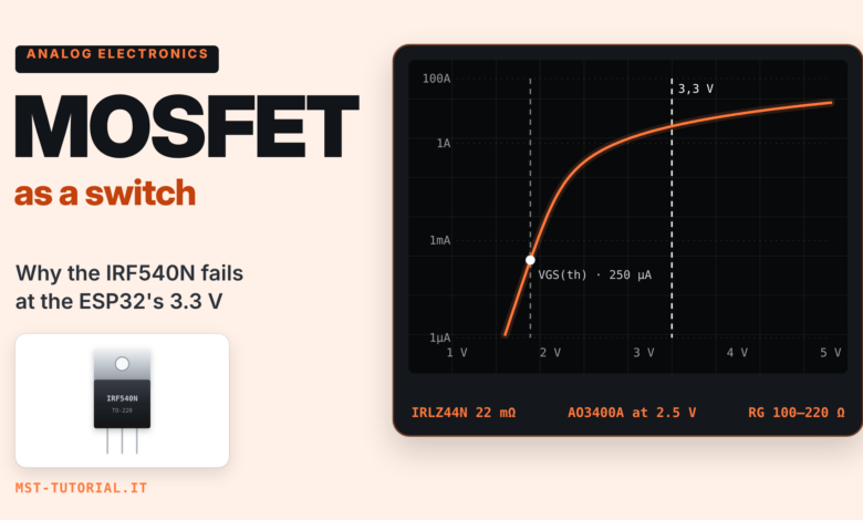
The MOSFET (Metal-Oxide-Semiconductor Field-Effect Transistor) is the component used in practice to switch on, switch off and PWM-control almost every DC load: the MOSFET as a switch drives LED strips, motors, fans, solenoid valves and heating resistors. Unlike the BJT transistor (in Italian), it is voltage-controlled rather than current-controlled, and when fully on it behaves like a resistance of a few milliohms: that is why it can switch tens of amperes while heating up very little.
The MOSFET does, however, have a few traps that catch people starting out with Arduino or ESP32 by surprise: the threshold voltage VGS(th) is not the voltage at which the device actually turns on, many “famous” models do not conduct well with a 5 V gate and almost none conduct well with the 3.3 V of the ESP32, and the gate behaves like a capacitor that must be charged and discharged at every transition. In this guide we cover structure and operating regions, the datasheet parameters with real data from four popular parts, low-side and high-side circuits, PWM losses, heat sink sizing with a complete numerical example, and the essential code for Arduino and ESP32.
MOSFET structure and symbols
A MOSFET has three terminals: gate (G), drain (D) and source (S). The gate is separated from the semiconductor by a very thin layer of silicon oxide: it is an insulator, so in steady state the gate draws no current (the leakage currents IGSS are on the order of 100 nA maximum). Gate, oxide and semiconductor effectively form a capacitor.
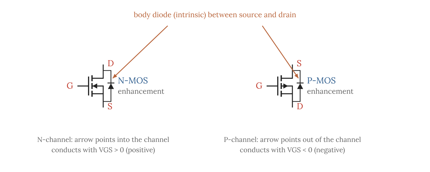
In the N-channel enhancement-mode MOSFET, the type used in nearly all power circuits, the substrate between source and drain is P-type (for a refresher on doping see N-type and P-type semiconductors (in Italian)). With the gate at 0 V there is no conductive path and the device is off. Applying a positive voltage between gate and source, the electric field across the oxide attracts electrons under the gate and forms an N channel that connects source and drain: the higher VGS, the “wider” the channel and the lower its resistance. The P-channel MOSFET works in the dual way: it conducts when the gate is more negative than the source, i.e. with VGS < 0.
Depletion-mode MOSFETs, which already conduct with VGS = 0, are not used for microcontroller switching and are not covered here.
The body diode
In vertical power MOSFETs the source is internally connected to the substrate (body). The PN junction between body and drain thus becomes an intrinsic diode that is always present and is drawn in the symbol: in the N-channel device it has the anode on the source and the cathode on the drain, in the P-channel device the anode on the drain and the cathode on the source. There are three practical consequences:
- a MOSFET blocks voltage in one direction only: if the drain of an N-MOS goes below the source, the body diode conducts whatever the gate voltage;
- the body diode can act as a freewheeling diode in H-bridges, but it is relatively slow and has a high forward drop (for the IRLZ44N
VSDis 1.3 V max at 25 A); - mounting the MOSFET “backwards” (drain and source swapped) produces a switch that stays permanently on through the diode.
Operating regions: cutoff, ohmic and saturation
The behavior of the MOSFET is read from the output characteristics ID–VDS, a family of curves, each at constant VGS. There are three regions.
- Cutoff:
VGSbelow the threshold, the channel does not exist and only the leakage currentIDSS(microamperes) flows. This is the “off” state of a switch. - Ohmic or triode region:
VGSwell above the threshold and smallVDS. The current rises almost linearly withVDS: the channel behaves like a resistance, theRDS(on), which is lower the higherVGSis. This is the “on” state of a switch. - Saturation region:
VDS > VGS − VGS(th). The channel pinches off at the drain end and the current becomes almost independent ofVDS, set byVGS. This is the region for amplifiers and current sources.
Watch the terminology, which is the main source of confusion: MOSFET saturation corresponds to the active region of the BJT, while BJT “saturation” (transistor fully on) corresponds to the MOSFET’s ohmic region. A MOSFET used as a switch must be in the ohmic region when it is on, not in saturation.

The curves in the figure are computed with the simplified square-law MOSFET model, using illustrative parameters; real values must always be read from the Typical Output Characteristics and Typical Transfer Characteristics graphs in the datasheet. In the saturation region the model gives:
\(I_D \approx \frac{K}{2}\left(V_{GS}-V_{GS(th)}\right)^2\)
Near the threshold, a few tenths of a volt on the gate change the current enormously: this is the region where a “standard” MOSFET driven at 3.3 V ends up.
Key datasheet parameters
For every quantity in the datasheet, also read the test condition, which often matters more than the number itself.
VDS and ID: maximum voltage and current
V(BR)DSS is the maximum drain-source voltage with the gate off. It must be chosen with margin over the supply voltage, taking into account the overvoltages caused by inductances: for a 12 V load a 30 V MOSFET is the reasonable minimum. The current ID in the table, on the other hand, is an almost theoretical figure: for the IRLZ44N it is 47 A at TC = 25 °C and 33 A at TC = 100 °C, i.e. with the case held at that temperature by an ideal heat sink. The current that can actually be sustained is determined by power dissipation and the heat sink, as we will see in the example.
VGS(th): why it is not the turn-on voltage
The threshold voltage is defined as the VGS at which a tiny drain current flows, with VDS = VGS: 250 µA for the IRLZ44N, IRF540N and AO3400A, just 25 µA for the IRLB8721. At the threshold the MOSFET is therefore “barely ajar”, not on. Moreover, it is given as a range (for the IRF540N from 2.0 to 4.0 V) and it decreases with temperature (the IRLB8721 states about −7 mV/°C).
The quantity that matters for a switch is a different one: the VGS at which the manufacturer guarantees the RDS(on). If the datasheet specifies RDS(on) only at 10 V, the part must be driven at 10 V; if it also specifies it at 4.5 V or 2.5 V, those are the guaranteed gate voltages.
RDS(on) at the stated VGS
The on-resistance determines the static losses, P = ID² · RDS(on). It must always be read together with the gate voltage and the test current, and corrected for temperature: RDS(on) increases with junction temperature, typically by 40–80 % between 25 °C and 125–150 °C. For the AO3400A, for example, the datasheet gives at 10 V a maximum of 26.5 mΩ at 25 °C and 38 mΩ at 125 °C (factor 1.43). The exact value is taken from the Normalized On-Resistance vs. Temperature graph.
Qg, Ciss and parasitic capacitances
The capacitances Ciss, Coss and Crss (Miller capacitance) are measured at VGS = 0 but vary a lot with voltage; for switching times the gate charge Qg is more useful: the amount of charge the drive circuit must supply to bring the gate from zero to the test voltage. It is split into Qgs (charge up to the plateau) and Qgd (Miller charge, supplied while the drain voltage falls): during the Qgd phase the gate voltage stays fixed at the plateau voltage, and that is where the MOSFET dissipates the most.
SOA and thermal resistances
The SOA (Safe Operating Area) is the ID–VDS graph on a logarithmic scale that bounds the voltage and current combinations the device can withstand for pulses of various durations and in DC (DC line). When switching, the MOSFET crosses the high-power area for very short times; it becomes critical, instead, when the MOSFET operates in the linear region for long periods (current limiters, electronic loads, soft-start, slowly driven gate).
The thermal data are the thermal resistances: RθJC junction-to-case, RθCS case-to-sink (with thermal paste), RθJA junction-to-ambient without a heat sink. Together with the maximum junction temperature (175 °C for the TO-220 parts considered here, 150 °C for the AO3400A) they allow the thermal calculation.
Four MOSFETs compared
The table lists the main data from the official Infineon (formerly International Rectifier) and Alpha & Omega datasheets, at TJ = 25 °C. For Qg and RDS(on) the test conditions are given.
| Parameter | IRF540N | IRLZ44N | IRLB8721 | AO3400A |
|---|---|---|---|---|
| Package | TO-220 | TO-220 | TO-220 | SOT-23 |
| V(BR)DSS | 100 V | 55 V | 30 V | 30 V |
| Continuous ID | 33 A (TC = 25 °C) | 47 A (TC = 25 °C) | 62 A (TC = 25 °C) | 5.7 A (TA = 25 °C) |
| VGS max | ±20 V | ±16 V | ±20 V | ±12 V |
| VGS(th) min–max | 2.0–4.0 V (250 µA) | 1.0–2.0 V (250 µA) | 1.35–2.35 V (25 µA) | 0.65–1.45 V (250 µA) |
| RDS(on) max | 44 mΩ at 10 V | 22 mΩ at 10 V 25 mΩ at 5 V 35 mΩ at 4 V |
8.7 mΩ at 10 V 16 mΩ at 4.5 V |
26.5 mΩ at 10 V 32 mΩ at 4.5 V 48 mΩ at 2.5 V |
| Qg | 71 nC max (VGS = 10 V) | 48 nC max (VGS = 5 V) | 7.6 nC typ. (VGS = 4.5 V) | 6 nC typ. (VGS = 4.5 V) |
| Typical Ciss | 1960 pF | 1700 pF | 1077 pF | 630 pF |
| RθJC / RθJA | 1.15 / 62 °C/W | 1.4 / 62 °C/W | 2.3 / 62 °C/W | RθJA 125 °C/W (on 1 in² of copper) |
| Gate from 5 V Arduino | No | Yes | Yes (reduced margin) | Yes |
| Gate from 3.3 V ESP32 | No | Not guaranteed | Not guaranteed | Yes |
Logic-level MOSFETs and the 3.3 V problem
A logic-level MOSFET is one whose RDS(on) is guaranteed at a gate voltage compatible with logic: 4.5–5 V for classic “logic level” parts, 2.5 V or less for very-low-threshold types. The table shows the typical case: the IRF540N, extremely popular in kits, is specified only at 10 V and with a threshold that can reach 4 V; at 5 V on the gate the manufacturer guarantees nothing and a given sample may stay half-on, heating up a lot. The IRLZ44N (the “L” in the part number stands precisely for logic-level gate) is guaranteed at 5 V and at 4 V, and is fine for an Arduino Uno.
With the ESP32 the problem moves lower. The Espressif datasheet guarantees an output VOH ≥ 0.8 · VDD, i.e. 2.64 V with a 3.3 V supply, at the specified load current. At that voltage the IRLZ44N and the IRLB8721 are just above their maximum threshold and their RDS(on) is not specified: some samples will work, others will dissipate watts instead of milliwatts. There are three correct solutions:
- a MOSFET with
RDS(on)guaranteed at 2.5 V, such as the AO3400A (48 mΩ max at 2.5 V and 3 A), suitable for loads of a few amperes; - a gate driver supplied at 10–12 V with a 3.3 V-compatible input, which brings the gate of a power MOSFET to the voltage at which it is specified (see below);
- a level shifter made with a transistor and a pull-up resistor to the load voltage, acceptable for slow switching.
Quick check for the AO3400A driven by an ESP32 with a 12 V, 2 A LED strip: with the maximum RDS(on) at 2.5 V corrected for temperature (48 mΩ · 1.43 ≈ 69 mΩ) it dissipates 2² · 0.069 ≈ 0.28 W; with an RθJA of 125 °C/W the junction reaches about 40 + 35 = 75 °C at 40 °C ambient. The RθJA value, however, only holds with the manufacturer’s copper test pad: on a printed circuit board with minimal traces the temperature will be higher.
MOSFET as a low-side switch (N-MOS)
The simplest and most widely used configuration is the low-side switch: the load is connected between the positive rail and the drain, and the source goes to ground. The N-channel MOSFET switches the “low side” of the load and the drive voltage is referenced to ground, so the GPIO can supply it directly.

Gate resistor
At the instant of switching, the discharged gate is almost a short circuit to ground: without a resistor, the peak current would be limited only by the internal resistance of the microcontroller output. The gate resistor RG limits the peak (with 150 Ω and 5 V about 33 mA in theory, less in practice because of the pin’s internal resistance) and damps the ringing formed by the wiring inductance and the gate capacitance. Typical values with direct GPIO drive: 100–220 Ω. A larger RG slows down switching and increases losses, as we will see in the calculation.
Pull-down resistor
During reset and firmware startup, GPIOs are high-impedance inputs. A floating gate can charge up through capacitive coupling or noise and partially turn on the MOSFET, which overheats in the linear region. The RPD resistor of 10–100 kΩ between gate and source keeps the MOSFET off until the microcontroller takes control; it should be placed close to the MOSFET, after RG. The voltage divider it forms with RG is negligible (150 Ω versus 10 kΩ: −1.5 %).
Flyback diode with inductive loads
A motor, a relay coil or a solenoid valve are inductances: when the MOSFET opens, the current cannot drop to zero instantly and the drain voltage rises until it finds a path (v = L · di/dt, see the in-depth article on inductors (in Italian)). Without protection it exceeds V(BR)DSS and drives the MOSFET into avalanche at every turn-off. The flyback diode D1, in antiparallel with the load with the cathode toward the positive rail, gives the current a path and clamps the drain voltage to about VCC + VF. The diode must handle the load current; for PWM a Schottky (in Italian) is preferable, being fast and having a low forward drop. The MOSFET’s body diode does not protect against this overvoltage: it is oriented so that it conducts only if the drain goes below the source.
Finally, the common ground: the microcontroller GND must be connected to the negative terminal of the power supply, otherwise the VGS voltage is undefined. The load current, however, must not flow through the ground traces of the logic board: the power return should be routed directly from the source to the negative terminal of the power supply.
High-side drive with a P-MOS and level shifting
Sometimes the load must stay connected to ground: a device whose chassis is grounded, a module whose negative is shared with other circuits, a powered sensor. In that case the high side is switched with a P-channel MOSFET: the source goes to the positive rail and the MOSFET conducts when the gate is pulled a few volts below the source. A 3.3 V or 5 V GPIO cannot do this directly: with 12 V on the source, a gate at 3.3 V would mean VGS = −8.7 V, i.e. the MOSFET is on even with the GPIO high. A level-shifting stage with an NPN (or a small N-MOS) is needed.

How it works: with the GPIO low, transistor Q1 is in cutoff, R1 pulls the gate to the source potential and the P-MOS is off. With the GPIO high, Q1 saturates and the gate is pulled toward ground through R2; R1 and R2 form a voltage divider that sets VGS ≈ −12 · 10/11 ≈ −10.9 V, within the ±20 V limit of the IRF9540N and beyond the −10 V at which its RDS(on) is specified (0.117 Ω max). The divider is essential with supplies above 15–20 V, where connecting the gate directly to ground would exceed the maximum VGS. The BJT is sized following the rules covered in the article on the NPN BJT transistor (in Italian):
Calculation example: level-shifting stage for high-side P-MOS
VCC = 12 V, R1 = 10 kΩ, R2 = 1 kΩ, GPIO = 3.3 V, Q1 = 2N3904

Q1 collector current:  IC ≈ 12 V / (10 kΩ + 1 kΩ) ≈ 1.1 mA
Gate voltage:          VGS ≈ -12 · 10 / 11 ≈ -10.9 V
Base current:          IB = (3.3 - 0.7) V / 4.7 kΩ ≈ 0.55 mA
Forced beta:           1.1 / 0.55 ≈ 2  -> Q1 saturated with ample margin
RBE = 100 kΩ: keeps Q1 off with a floating GPIO (draws about 7 µA)

Turn-off: the gate recharges only through R1 = 10 kΩ
Initial current 12 V / 10 kΩ = 1.2 mA; Qg max 97 nC
t_off on the order of Qg / I ≈ 97 nC / 1.2 mA ≈ 80 µs
-> suitable for ON/OFF or PWM at a few hundred Hz, not at 20 kHz
The logic is not inverted: GPIO high means load on. The slow turn-off depends on R1: lowering it speeds things up but increases Q1’s current while the load is on. For a fast high-side switch or for high currents, a push-pull stage on the gate or an N-MOS with a bootstrap driver is used.
PWM and switching losses
In PWM the MOSFET alternates between conduction and cutoff at a fixed frequency, and the average power delivered to the load is proportional to the duty cycle D (see analog inputs and PWM outputs with Arduino (in Italian)). The MOSFET losses are the sum of two terms.
The conduction losses depend on the RMS value of the current; with a resistive load and constant current during conduction:
\(P_{cond} = I_D^2 \cdot R_{DS(on)} \cdot D\)
The switching losses arise because, during each transition, voltage and current are both nonzero at the same time. The most commonly used estimate is the one for an inductive load with a freewheeling diode, in which during each transition the voltage stays at its full value until the current has been commutated; with a purely resistive load, where voltage and current change together, the actual losses are about one third, so the formula is conservative:
\(P_{sw} \approx \frac{1}{2} V_{DS} \, I_D \left(t_{on}+t_{off}\right) f_{PWM}\)
The transition times are estimated from the gate charge and the current the drive circuit can deliver during the plateau. The charge that matters is the one spent while voltage and current swap over, approximated by Qsw ≈ Qgd + Qgs/2:
\(I_{G,on} \approx \frac{V_{drv}-V_{plateau}}{R_G} \qquad I_{G,off} \approx \frac{V_{plateau}}{R_G} \qquad t \approx \frac{Q_{sw}}{I_G}\)
The plateau voltage is read from the Gate Charge graph in the datasheet; for a logic-level MOSFET it is typically between 2.5 and 3.5 V. With a 5 V GPIO and 150 Ω the gate current during the plateau is about 13–20 mA and switching takes microseconds; with a gate driver of a few amperes it takes tens of nanoseconds. The following graph, computed with this formula (conservative estimate) for the example in the next section, shows the effect of the PWM frequency.
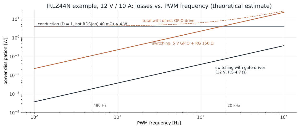
At the standard Arduino Uno PWM frequency (490 Hz, 980 Hz on pins 5 and 6), the switching losses with direct drive are negligible compared with the conduction losses. At 20 kHz, a frequency often chosen to make motor PWM inaudible, they become larger than the conduction losses: that is the sign that a gate driver is needed.
When a gate driver is needed
A gate driver charges and discharges the gate with peaks of several amperes and, supplied at 10–12 V, brings VGS to where RDS(on) is lowest. It is needed when:
- the PWM frequency exceeds a few kHz with power MOSFETs (
Qgof tens of nC); - the microcontroller runs at 3.3 V and the MOSFET suitable for the required current is not specified at 2.5 V;
- the current is high and you want the
RDS(on)at 10 V instead of the one at 4.5 V; - the MOSFET is in an N-channel high-side configuration or in an H-bridge (driver with bootstrap).
An example of a low-side driver is the Texas Instruments UCC27517: 4 A peak output, 4.5 to 18 V supply, input high threshold of 2.2 V typical (2.4 V max) independent of the supply, and therefore compatible with a 3.3 V GPIO. It requires a ceramic decoupling capacitor close to the supply pin.
Complete example: power dissipation and heat sink
Example design: an Arduino Uno drives, with 490 Hz PWM, a 12 V, 10 A (120 W) heating resistor through an IRLZ44N in low-side configuration, RG = 150 Ω, ambient temperature inside the enclosure 40 °C. The worst case is sized, D = 1 (load always on).
Calculation example: IRLZ44N, 12 V / 10 A, 5 V gate, 490 Hz PWM

1) Checks against maximum ratings
   V(BR)DSS = 55 V > 12 V                       -> OK, ample margin
   ID = 10 A << 33 A (TC = 100 °C)               -> OK
   VGS = 5 V < 16 V                             -> OK

2) Conduction losses (D = 1)
   RDS(on) max at VGS = 5 V, 25 °C:  25 mΩ
   Assumed temperature factor (TJ ≈ 100-125 °C): 1.6
   Hot RDS(on) = 25 · 1.6 = 40 mΩ
   Pcond = 10² · 0.040 = 4.0 W

3) Switching losses
   Qsw ≈ Qgd + Qgs/2 = 25 + 8.6/2 ≈ 29.3 nC   (max values at VDS = 44 V: conservative estimate)
   Assumed Vplateau ≈ 3 V
   IG,on  = (5 - 3) / 150 ≈ 13.3 mA  -> t_on  ≈ 29.3 nC / 13.3 mA ≈ 2.2 µs
   IG,off = 3 / 150 = 20 mA          -> t_off ≈ 29.3 nC / 20 mA  ≈ 1.47 µs
   Esw = 0.5 · 12 · 10 · (2.2 + 1.47) µs ≈ 220 µJ per period
   Psw = 220 µJ · 490 Hz ≈ 0.11 W      (at 20 kHz it would be 4.4 W)

4) Total power
   Ptot ≈ 4.0 + 0.11 ≈ 4.1 W
   (power in the gate circuit Qg·Vdrv·f = 48 nC · 5 V · 490 Hz ≈ 0.1 mW: negligible)

5) Without a heat sink
   TJ = TA + Ptot · RθJA = 40 + 4.1 · 62 ≈ 295 °C   -> IMPOSSIBLE (max 175 °C)

6) Required heat sink (target TJ ≤ 110 °C, margin below 175 °C)
   Rth,tot max = (110 - 40) / 4.1 ≈ 17 °C/W
   RθSA max = 17 - RθJC - RθCS = 17 - 1.4 - 0.5 ≈ 15 °C/W
   with insulating pad (about +1 °C/W):  RθSA ≤ 14 °C/W

7) Check with a commercial 10 °C/W heat sink
   TJ = 40 + 4.1 · (1.4 + 0.5 + 10) ≈ 89 °C   -> OK; at about 90 °C the 1.6 factor is conservative
The thermal calculation follows the “thermal Ohm’s law”, with thermal resistances in series:
\(T_J = T_A + P_{tot}\left(R_{\theta JC}+R_{\theta CS}+R_{\theta SA}\right)\)
With a 12 V gate driver, RDS(on) would drop to 22 mΩ max (10 V), i.e. 3.5 W hot instead of 4.0, with negligible switching losses even at 20 kHz. Often, though, a lower-resistance MOSFET is the better choice: with the IRLB8721 (16 mΩ max at 4.5 V) conduction losses drop by about one third.
PWM code for Arduino and ESP32
On the Arduino Uno, analogWrite() is all you need, with values from 0 to 255 on pins 3, 5, 6, 9, 10, 11. Drive the pin low right away in setup(), even though the pull-down already keeps the MOSFET off during reset.
// Arduino Uno: PWM on a low-side MOSFET (pin 9 = Timer1, 490 Hz)
const uint8_t PIN_GATE = 9;

void setup() {
  pinMode(PIN_GATE, OUTPUT);
  digitalWrite(PIN_GATE, LOW);      // load off at startup
}

void loop() {
  for (int d = 0; d <= 255; d++) { // ramp from 0 % to 100 %
    analogWrite(PIN_GATE, d);
    delay(10);
  }
  delay(1000);
  analogWrite(PIN_GATE, 0);
  delay(1000);
}
You can raise the frequency of pins 9 and 10 to about 31.4 kHz (16 MHz / 510) with TCCR1B = (TCCR1B & 0b11111000) | 0x01;, but the change interferes with libraries that use Timer1 (for example Servo) and, above all, with direct GPIO drive the previous example would dissipate about 7 W in switching alone.
On the ESP32 with Arduino core 3.x the LEDC API has changed compared with version 2.x: channels are assigned automatically and the functions work on the pin number. ledcAttach(pin, frequency, resolution) configures the pin and ledcWrite(pin, duty) sets the duty cycle; the old ledcSetup() + ledcAttachPin() scheme no longer exists. The maximum resolution depends on the frequency: with the 80 MHz clock, at 20 kHz you get up to 11 bits (80 MHz / 20 kHz = 4000 ≈ 211.97).
// ESP32, Arduino core 3.x: 20 kHz PWM, 10-bit resolution
const uint8_t  PIN_GATE = 18;
const uint32_t PWM_FREQ = 20000;   // 20 kHz: only with a gate driver or a low-Qg MOSFET
const uint8_t  PWM_RES  = 10;      // duty from 0 to 1023

void setup() {
  Serial.begin(115200);
  if (!ledcAttach(PIN_GATE, PWM_FREQ, PWM_RES)) {
    Serial.println("LEDC configuration error");
  }
  ledcWrite(PIN_GATE, 0);          // load off
}

void loop() {
  for (uint32_t d = 0; d <= 1023; d += 8) {
    ledcWrite(PIN_GATE, d);
    delay(10);
  }
  delay(1000);
  ledcWrite(PIN_GATE, 0);
  delay(1000);
}
Alternatively, core 3.x also offers an Arduino-compatible analogWrite(pin, value) (0–255), with analogWriteFrequency() and analogWriteResolution() to change frequency and resolution. Remember that at 3.3 V the MOSFET must be specified at 2.5 V, or a gate driver must be added.
Comparison with BJT, IGBT and relay
| Device | Drive | On-state drop | Speed | Typical use |
|---|---|---|---|---|
| BJT | Current (continuous base current) | VCE(sat) 0.1–1 V |
Good for small signals | Small loads up to a few hundred mA, level shifters |
| MOSFET | Voltage (current only during transitions) | ID · RDS(on), as low as a few mV |
Very high (ns) | DC loads up to tens of A, PWM, low- and medium-voltage converters |
| IGBT | Voltage, typically 15 V | VCE(sat) 1.5–3 V |
Medium (tail current) | High voltages and power: inverters, motor drives, welders |
| Relay | Coil (needs a transistor) | Contact resistance, no threshold | Slow (ms), limited mechanical life | Galvanic isolation, AC loads, infrequent switching |
For DC loads of a few amperes the MOSFET is almost always the best choice. The BJT (in Italian) remains handy as a level shifter or for small loads, the IGBT (in Italian) wins above a few hundred volts, and the relay is needed when isolation is required or when switching mains, as described in controlling AC loads with Arduino or Raspberry (in Italian).
Common mistakes
- Choosing the MOSFET based on
VGS(th): a 2 V threshold does not mean the MOSFET is on at 3.3 V. What matters is theVGSat whichRDS(on)is guaranteed. - Using the IRF540N, IRFZ44N or similar with a 5 V or 3.3 V gate: they are specified at 10 V. The circuit seems to work with no load and heats up under load.
- Floating gate: without a pull-down the MOSFET can partially turn on at power-up or with the GPIO wire disconnected.
- Forgetting the flyback diode with motors, relays and solenoid valves, relying on the body diode, which does not come into play.
- Ground not shared, or shared at the wrong point: load current flowing through the logic board’s ground shifts the references and causes resets and wrong readings.
- Trusting the ID in the table: without a heat sink a TO-220 can handle about 1–2 W, not 47 A.
- High-side mounting with an N-MOS and a 5 V gate: the source rises to about
VG − VGS(th), the load gets only a few volts and the MOSFET operates in the linear region, dissipating the rest. - Exceeding the maximum
VGS(±12 V for the AO3400A, ±16 V for the IRLZ44N) with gate drivers or voltage dividers supplied from the load voltage; if there are transients on the gate, add a gate-source protection Zener (in Italian).
Design checklist: MOSFET as a switch for a microcontroller

 1. V(BR)DSS >= 2 x supply voltage (inductive overvoltages).
 2. RDS(on) guaranteed at the VGS actually available:
    5 V -> specified at 4.5 V or 4 V;  3.3 V -> specified at 2.5 V
    (or a gate driver).
 3. Pconduction with hot RDS(on) (x 1.5-1.8) and RMS current.
 4. Pswitching from Qg, gate current and PWM frequency.
 5. TJ = TA + P · total Rth with margin below 150-175 °C.
 6. RG 100-220 Ω from GPIO, pull-down 10-100 kΩ gate-source.
 7. Flyback diode on every inductive load.
 8. Common ground, power return separate from logic ground.
 9. Fuse on the load supply line.
10. Maximum VGS never exceeded (drivers, voltage dividers, transients).
Sources and further reading
- Infineon IRLZ44NPbF, datasheet
- Infineon IRF540NPbF, datasheet
- Alpha & Omega Semiconductor AO3400A, datasheet
- Espressif, Arduino-ESP32: LED Control (LEDC) API
- Texas Instruments UCC27517, datasheet
Related articles
- PNP transistor as a high-side switch
- ATmega328P timers on Arduino
- NPN BJT transistor: operation, biasing and switching (in Italian)
- IGBT: structure, operation and applications (in Italian)
- Controlling AC loads with Arduino or Raspberry Pi (in Italian)
- How to use analog inputs and PWM outputs with Arduino (in Italian)
- Schottky diodes: structure, operation, applications (in Italian)